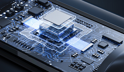
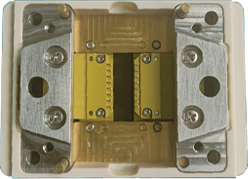
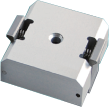
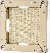
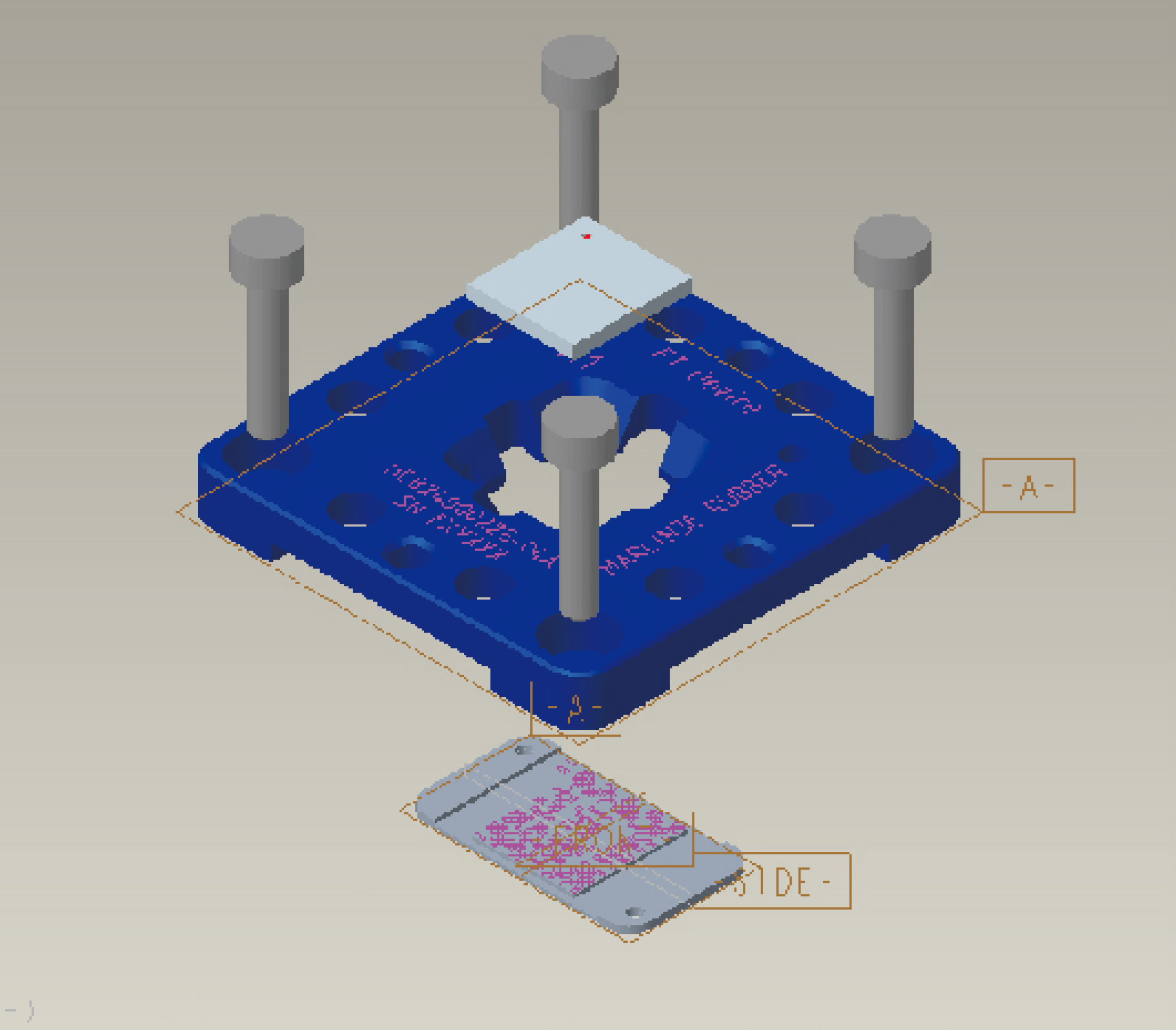
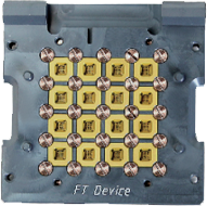
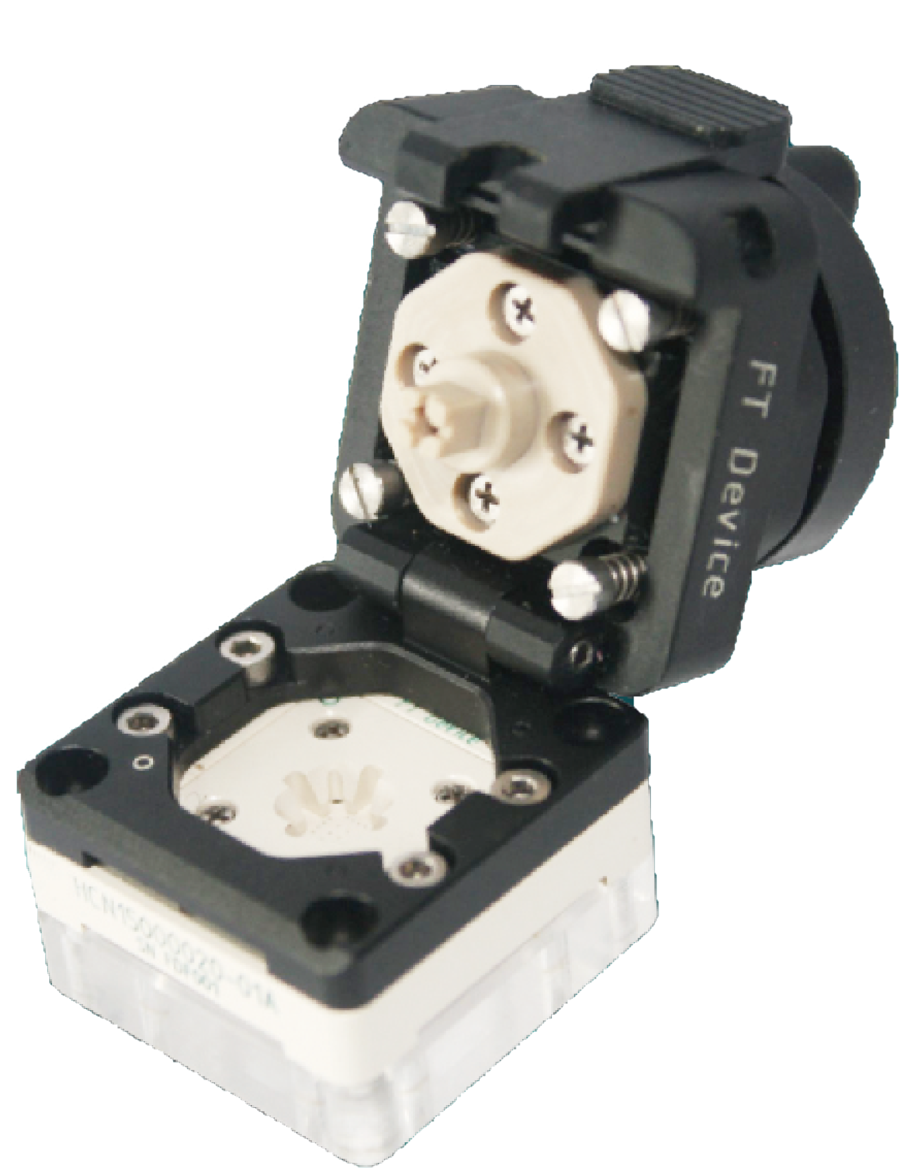
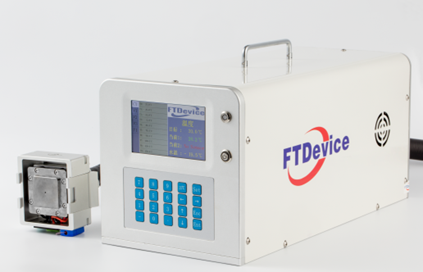
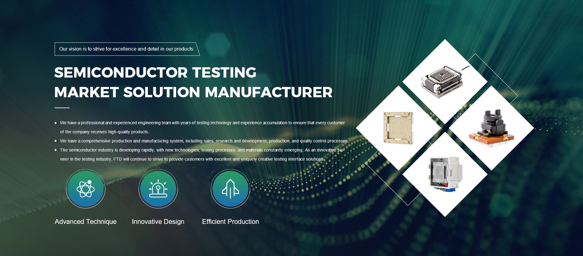
FT Device Technology (Suzhou) Co., Ltd Welcome~

Homepage > Priduct Display > High Performance

High Performance

Low Cost,high performance chip standard socket for mass production,

Significant contact resistance stability and long production life 

Standardized family design,simple and durable,best performance and low cost 

Multiple packages design 

Design for manual test, machine test and burn-in test. 

Shortest design and production cycle time


Contact Us
Introduce

Using FTD family standard sockets and lids allows for expediting design and delivery of our products. By utilizing design templates, socket and lid drawings for specific packages can be quickly completed. FTD family standards will allow products to have the same dimensioning features and overall look among multiple packages.


Key Feature

● Standard family design and best test performance 

● WLCSP,BGA,QFN,QFP multiple packages 

● 0.35mm lead pitch 

● Optimized positioning frame design 

● Excellent contact reisitance and current capability 

● Three temperature test capability(-40°C-150°C)

Package type

● Ball aray packages:BGA, LGA, WLCSP, others – 350 µm pitch and up

● Lead package: QFP, SO, others – 350 µm pitch and up

● Leadless package: QFN, others – 350 µm pitch and up

Mechanical

● Lead pitch: >0.35mm 

● Pin force: 15g -40g

● Test travel:0.3mm -0.65mm

Reliability

● Pin life:500K-1KK 

● Socket Life: >5KK

● Clean frequency:50K-100K

Materials

● Socket material: Vespel SP-1, Plavis – N, MDS-100, and Peek ceramic and others 

● Spring pin material: Gold PD


Electrical

● Contact resistance:50mΩ

● Current capacity:5A continous current 

● Bandwidth: > 20GHZ @-1db

● Inductance: 1.2nH

Environment

● Temperature range: -40°C - 150°C

Online message

Company Profile News Products Service Support Contact Us

Phone:+86-0512-6957 2000

Fax:+86-0512-6957 3000

Mailbox:kevin@ftdevice.com

Address:No. 200 Xingpu Road, SIP Suzhou, Jiangsu P.R.C

COPYRIGHT 2019 ALL 苏ICP备15011493号-1

技术支持:万禾网络